-
-
-
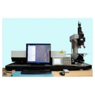
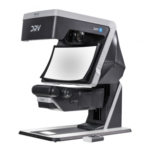
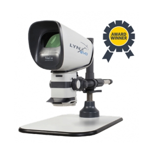
激光單粒子效應SEE測試儀
- 品牌:ASP
- 型號: SEE
- 產地:美洲 美國
- 供應商報價:面議
-
似空科學儀器(上海)有限公司
 更新時間:2025-04-25 20:23:31
 -
銷售范圍售全國
入駐年限第8年
營業執照已審核
- 同類產品芯片SEE激光模擬(1件)
立即掃碼咨詢
聯系方式: 4008558699轉8071
聯系我們時請說明在儀器網(www.shangjinews.cn)上看到的!
掃 碼 分 享 -
為您推薦
產品特點
- 單粒子效應對應用于航天以及核工業的芯片往往造成極大危害,相對于傳統的粒子加速器而言,利用脈沖激光進行檢測可以極大地提GX率,降低成本。以下型號型號激光SEE測試儀已經被應用于美國波音公司和NASA。
詳細介紹
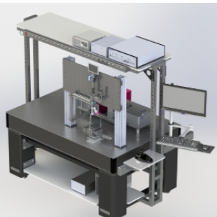
We offer custom SEE laser testing solutions:
Single photon
Two photons
Selection of Pico and Femto second lasers
Shortwave 900nm to 1700nm and Visible imaging system
Microscope objective choices; 200X, 100X, 50X 20X
Additional Features:
High accuracy X-Y-Z motorized stages ( nm resolution) 50mm travel XYZ, 0.1micron resolution
Joystick for X-Y
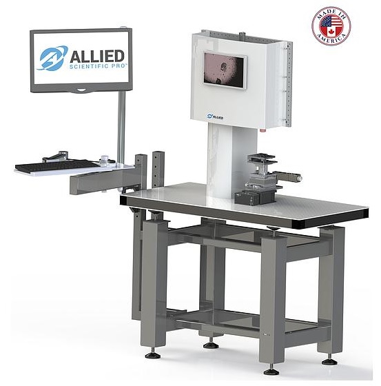 ?
?Tilt stat ( 3 rotation axes) manual micrometer or motorized
Protective enclosure
Dual microscope objective top and bottom (optional)
Replace Synchrotron beam-line time and high cost
For space, military, aerospace, Railways, Automotive, Avionic
Applications:
SEU: Single Event Upset
SET: Single Event Transient
SEL: Single Event Latch-up
SEGR: Single Event Gate Rupture
SEB: Single Event Burnout
SEGR: Single Event Gate Rupture
SEFI: Single Event Functional Interrupt
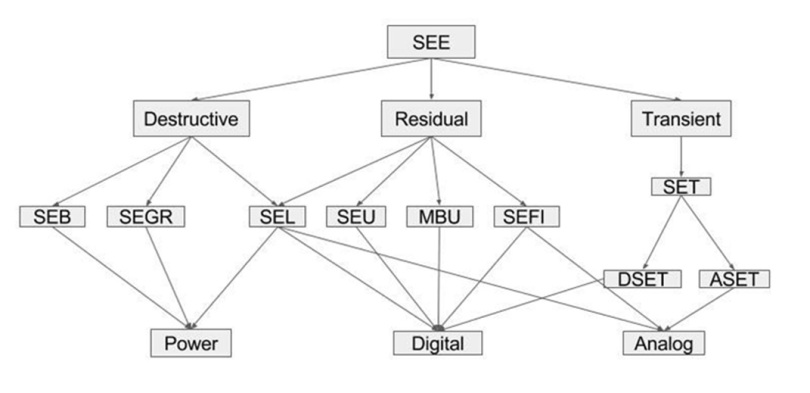
Single‐Event Effect (SEE): Any measurable or observable change in state or performance of a microelectronic device, component, subsystem, or system (digital or analog) resulting from a single energetic particle strike.
Single‐Event Transient (SET): A soft error caused by the transient signal induced by a single energetic particle strike.
Single‐Event Latch‐up (SEL): An abnormal high‐current state in a device caused by the passage of a single energetic particle through sensitive regions of the device structure and resulting in the loss of device functionality. SEL may cause permanent damage to the device. If the device is not permanently damaged, power cycling of the device (off and back on) is necessary to restore normal operation. An example of SEL in a CMOS device is when the passage of a single particle induces the creation of parasitic bipolar (p‐n‐p‐n) shorting of power to ground. Single‐Event Latch‐up (SEL) cross‐section: the number of events per unit fluence. For chip SEL cross‐section, the dimensions are cm2 per chip.
If the charge generated by a single high LET particle is collected by a single high LET particle is collected by a sensitive node of the device or circuit, and this charge is larger than the critical charge required to start an anomalous behaviour an effect singe even effect, may be seen affecting the electrical performance of the device or circuit such as soft errors or hard destructive errors. Space systems often require electronics that can operate in a high-radiation environment. This radiation may result from particles trapped in planetary magnetic fields (e.g., the Van Allen belts which affect Earth-orbiting satellites or the intense radiation fields of Jupiter and its moons), galactic cosmic rays, or high-energy protons from solar events. At low Earth orbit, an integrated circuit may be exposed to a few kilorads of radiation over its useful lifetime, while at orbits in the middle of the Van Allen belts, exposure levels may increase to several hundred kilorads or more. In addition to the natural space environment, military satellites must be able to survive transient bursts of radiation resulting from a hostile nuclear explosion. To achieve these higher levels, radiation-hardened integrated circuits are required. In general, these circuits are fabricated using specialized processes and designs that increase their tolerance to ionizing radiation by several orders of magnitude.
Semiconductor Failures
The primary effects of natural space radiation on spacecraft electronics are total ionizing dose (TID) and single event effects (SEE). TID creates bulk-oxide and an interface-trap charge that reduces transistor gain and shifts the operating properties (e.g., threshold voltage) of semiconductor devices. TID accumulation will cause a device to fail if (1) the transistor threshold voltage shifts far enough to cause a circuit malfunction, (2) the device fails to operate at the required frequency, and/or (3) electrical isolation between devices is lost. SEE occurs when a cosmic ray or other very high-energy particle impinges on a device. The particle generates a dense track of electron-hole pairs as it passes through the semiconductor, and those free carriers are collected at doping junctions. The net effect is that the circuit is perturbed and may lose data (called a single-event upset or SEU). The passage of a sufficiently energetic particle through a critical device region can even lead to permanent failure of an IC due to single-particle-event latchup (SEL), burnout, or dielectric/gate rupture. In general, components that exhibit SEL are not acceptable for space applications unless the latchup can be detected and mitigated. Burnout and gate rupture are especially problematic for high-voltage and/or high-current electronics associated with space-borne power supplies. SEE have become an increasing concern as ICs begin to use smaller device geometries and lower operating voltages, leading to reduced nodal capacitance and charge stored on circuit nodes. In addition to these primary effects, displacement damage effects caused by high-energy protons and electrons can reduce mission lifetimes due to long-term damage to CCDs, optoelectronics, and solar cells.
Radiation Protection
Radiation-hardened technology is often characterized as technology in which the manufacturer has taken specific steps (i.e., controls) in materials, process, and design to improve the radiation hardness of a commercial technology. Consider the case of CMOS technology, whose low power and voltage requirements make it a popular candidate for space applications. The most likely failure mechanism for CMOS devices resulting from TID is a loss of isolation caused by parasitic leakage paths between the source and drain of the device. For improved TID hardness, changes in the isolation structure may be required, e.g., a heavily-doped region or "guardband" can be formed by ion implantation that effectively shuts off radiation-induced parasitic leakage paths. In addition, a low thermal budget and minimum hydrogen during processing has been found to improve TID hardness. The use of oversized transistors and feedback resistors, capacitors, or transistors can be implemented for improved SEE immunity. For improved latchup and transient immunity, the change can sometimes be as simple as use of a thin epitaxial substrate. SOI technology that employs an active device layer built on an insulating substrate can (with proper design) provide significant improvement in SEE and transient tolerance. There are also several design approaches that can be used to increase radiation hardness. One global design change is the conversion of dynamic circuitry to full static operation, thereby placing data in a more stable configuration that is less susceptible to the perturbing effects of radiation. For TID, n-channel transistors can be designed in "closed" geometry that shuts off parasitic leakage paths. For SEU, memory cells with additional transistors can provide redundancy and error-correction coding (ECC) to identify and correct errors. Design approaches for improved radiation hardness generally result in a performance and layout area penalty. Unless specific steps such as these are taken during the design and manufacture of a device, radiation hardness levels are typically low and variable.
Non-Hardened Too
Unhardened, commercial CMOS circuits are typically able to withstand TID levels in the range from 5 to 30 kilorads at space-like dose rates. (The commonly used unit of TID is the rad, i.e.,radiation absorbed dose. One rad is equal to an adsorbed energy of 100 ergs per gram of material.) However, there are many space missions in which commercial CMOS technology may be used. In these missions (e.g., low Earth orbit), the spacecraft may be exposed to only a few kilorads of TID during its lifetime. As an example, Space Station Freedom may require integrated circuits with hardening requirements ranging from a few to 20 kilorads depending on platform location. In these applications, shielding and careful screening of technology (to take advantage of annealing in the space environment) enables the use of some unhardened, commercial technology. Historically, bipolar circuits have been very tolerant to total ionizing dose. Recently, major advances in bipolar technology have been due, in part, to the introduction of "recessed oxides." The recessed oxide lateral dielectric isolation acts as a diffusion stop, and minimizes junction capacitances. Thus, recessed oxides allow much smaller feature size, increased packing density, and higher speed. However, when irradiated, several parasitic leakage paths can be formed including buried layer to buried layer channeling, collector to emitter channeling on walled emitters, and increased sidewall current. The increased current associated with inversion of these parasitic MOS field transistors can lead to bipolar circuit failure at doses as low as 10 kilorads. Although bipolar technology offers speed advantages, its relatively high power consumption makes it less desirable than CMOS for most space applications. In the past few years, some bipolar circuits have been shown to exhibit ELDRS, an enhanced low-dose rate sensitivity that results in lower radiation tolerance for devices at space-like dose rates than indicated by higher dose-rate laboratory testing. CMOS circuits are generally the least sensitive to SEU due to the presence of active devices which restore the original voltage level of a node following a voltage transient induced by a heavy-ion strike. Combined with their low power requirements, CMOS circuits are often the choice for space applications. Still, unhardened CMOS SRAMs may experience upsets at a rate of 10-5 to 10-3 errors/(bit-day), which represents an upset every hour for a satellite with a large memory element in low-Earth orbit that passes through the South Atlantic Anomaly, an area of exceptionally high proton density that overlies much of South America and the South Atlantic Ocean.
DRAM Sensitivity
Dynamic circuits are generally very sensitive to SEU and are not used in critical space applications. In dynamic circuits, such as DRAMs (dynamic random access memories) and CCDs (charge coupled devices), information is represented as charge stored on a circuit node. In DRAMs this charge gradually leaks off the storage node and must be refreshed periodically. Upset in these devices occurs if sufficient charge is collected at a struck node to compensate the original stored charge. Although DRAMs and CCDs are not recommended for critical circuit applications, they have found increasing use in solid state data recorders and imaging systems where robust ECC can restore corrupted data. Bipolar devices are generally less sensitive to SEP than dynamic circuits, but more sensitive than MOS devices. Bipolar devices depend on steering of current within the circuit rather than charge storage to represent the binary state of memory elements. There are multiple charge collection regions associated with the emitter, base, collector, and substrate regions of the transistors, and each of these regions can have a different critical charge for upset. In some regions, transistor bases for example, charge is amplified by the normal operation of the device. A single ion can penetrate multiple sensitive regions resulting in synergistic effects between upset mechanisms for each region. The natural space radiation environment presents a great challenge to present and future satellite systems with significant assets in space. Defining the requirements for such systems demands knowledge about the space radiation environment and its effects on electronics and optoelectronics technologies, as well as suitable risk assessment of the uncertainties involved. For missions with high radiation levels, radiation-hardened integrated circuits will be required to perform critical mission functions. The most successful systems in space will be those that are best able to blend standard commercial electronics with custom radiation-hardened electronics in a mix that is suitable for the system of interest. Extracted from an article from Peter S. Winokur, at the Sandia National Laboratories.
What should I use for: Heavy ions Laser Single photon Two-photon Screening devices with different designs in the same technology node for SEU-MBU + ++ (+) Accurate SEU cross section vs LET measurement for a memory device ++ Testing fault-tolerant system level solutions + ++ + Analyzing deep charge collection mechanisms + + (++) Mapping SEL sensitive area of a flip-chip device + ++ Validating an SEL-free design ++ + Studying rare SEFI events in a recent digital devices ++ ++ Validating the radiation hardening efficiency of a design update + ++ + Obtain 3D view of charge collection volumes